Background
I want to keep record of a debugging experience for cache coherence problem on the ARM cortex-A57 platform for future reference. We had a project for hardware-based memory management for hybrid memory systems (fast expensive DRAM + slow but cheap NVM). The hardware platform we are using is an EMC customized board with an 8 core ARM A57 connected with FPGA controlled DIMMs through PCIe bus as shown in Figure 1. The memory management logic is implemented in FPGA. The ARM chip serves as host to run applications. We assume in the future, the processor will have extra logic along with the memory controller for DRAM and NVM to implement some page/sub-page movement policy between DRAM and NVM.
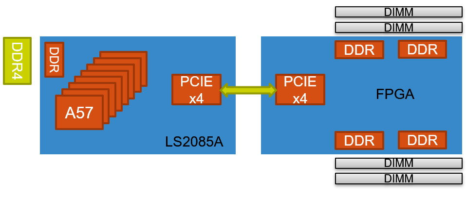 |
|---|
| Figure 1 Platform diagram |
I was responsible for the host side, i.e. mapping the application memory allocate to the I/O memory (PCIe bar memory). We developed a customized driver to make the memory-mapped IO cacheable and modified jemalloc to hook up with the application code. The other student works on the RTL to implement the policy of page movement between two tiers of memory. As the project develops, we might a lot of issues when running the real applications (SPEC 2006). I always think the problems belong to hardware implementation issues since there are a lot of changing going on during that time. However, after several months past, the system is still not stable.
Software code path
In order to port the process memory (mainly heap memory) from host side DRAM to I/O memory (FPGA controlled DRAM, communicate with host through PCIe 3.0), way mainly add two pieces of software layer.
-
Customized heap allocator. We modified jemalloc and override the glibc library for memory allocation (malloc and new for c/c++). Instead of using brk and mmap (anonymous pages) to allocate heap memory from the operating system, we use mmap to allocate memory from our customized driver to map memory-mapped I/O memory.
-
Customized driver. We implemented a simple driver to manage memory allocation from memory-mapped I/O memory (FPGA memory). The driver mainly does two things. First, it does bookkeeping of the dynamic memory allocation from the library side using Linux gen_pool_alloc interface (bitmap allocation). The bookkeeping is at chunk base (2MB granularity). We also implemented a linked-list to keep track of all allocated chunks for error handling, so that user space mistake won’t mess up with the system. Second, it marks the allocated chunks cacheable when setting up the page table (when user space call mmap).
The slow code path for application allocation will go through library call malloc, then mmap call to the driver to get large piece of memory. After driver finishing bookkeeping and error checking, it set up the page table for the allocated pages and return to the user space.
Problem Description
The problem looks like this. The applications (SPEC 2006) sometimes can finish successfully, sometimes fails with error, sometimes produce the incorrect results. Another special phenomenon is after the full power cycle of the system, the first application has a higher correct rate. Based on this, we decided to do an in-depth debugging which also includes the software path.
How to Debug
We prepared a minimum HW/SW system and try to reproduce the error with minimum effort. The reason behind that is we can spare FPGA logic and use the FPGA debugging tool (chipscope/signaltap) to capture real memory traces (PCIe TLP requests from LLC). I wrote a simple c program that mimicks a memory test application and jemalloc behavior (the driver is quite simple, first using __pgprot_modify to make the mmapped PCIe bar memory cacheable, then using remap_pfn_range to setup the page table) for accessing the memory. Since the LLC may absorb most of the access that cannot expose the memory transactions to the hardware (FPGA side). I explicitly flush the cacheline for every memory access from the c test program. (The cacheline flush is implemented in kernel space with inline assembly). The memory test logic is similar to x86 memtest program that write various data patterns and read back for comparison. (This memory test program is able to trigger the problem we observed previously, but with a lower rate compared to SPEC2006.) The micro testing program also contains triggering logic for FPGA signaltap trigger and error checking (stop signaltap). However, since we bypass host side cache, the error rate is much higher and can easily trigger memory error.
After launch the simulated program (that emulate the entire software stack) many times. We were able to trigger a memory error (from the memory test logic). We then collect memory traces from the FPGA side. I manually analyze the memory traces to find what is the root cause events.
The bug we found
While examining the memory traces to the FPGA (basically LLC misses, or PCIe memory requests), I found the memory event that cause the memory error (RAW) and finally revealed the issue that dangled for the past few months.
From the trace, I located the error memory address (report from the user-space memory checker program) and trace back the memory traffic before that access. I found there are duplicated writes to that address that eventually cause the problem. So, a write with stale data in between a read after write (RAW) sequence which triggers the software error. This indicates that it might be a dirty cacheline write back event from another core that corrupts the correct data (the memory address that has error). It is highly possible there is an I/O coherency bug that is the root cause of this issue.
A few months later, we were able to talk with some folks from Intel. One of them were in the FPGA team (Altera) for a while and confirm this bug. What an experience!